
Beauty Elevate
Hacking A Digital Microscope Camera For Fun And Automated PCB Inspection
Jun
Note: This article is written for educational, maker, and electronics-inspection purposes. “Hacking” here means creatively modifying your own hardware, software, and workflownot doing anything shady enough to require a fake mustache.
When a Digital Microscope Becomes More Than a Fancy Magnifying Glass
A digital microscope camera is one of those tools that feels slightly magical the first time you use it. One minute you are squinting at a tiny solder joint like a jeweler who forgot their coffee; the next, a 0.5 mm pitch IC is glowing on your monitor like a movie star on a red carpet. For electronics hobbyists, repair technicians, PCB designers, and small-batch manufacturers, that alone is worth the price of admission.
But the real fun begins when the microscope stops being a passive viewer and becomes part of an automated inspection system. Instead of only looking at a printed circuit board by hand, you can capture images, move the board under software control, compare regions against known-good references, detect suspicious solder joints, and document results. That is where hacking a digital microscope camera turns from weekend tinkering into a surprisingly practical machine-vision project.
The idea is simple: take an affordable USB or HDMI digital microscope, connect it to a computer or single-board system, add repeatable movement and lighting, then use software to inspect PCB features. The execution, naturally, is where the adventure lives. Focus drifts. Cheap lenses distort. LEDs create glare. The camera driver hides useful settings. The PCB refuses to sit perfectly flat because apparently even fiberglass has opinions. Still, with a few smart choices, a low-cost digital microscope can become a useful automated PCB inspection station.
Why PCB Inspection Needs Better Eyes
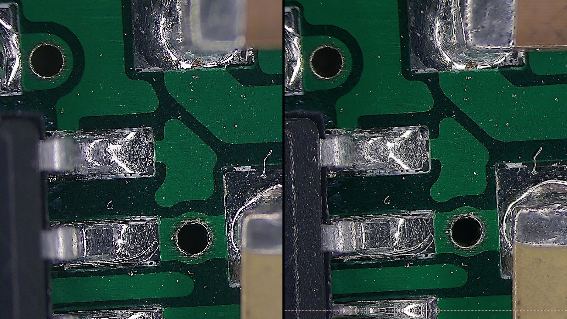
Modern PCBs are dense, compact, and full of parts that look like crumbs from a robot bakery. Surface-mount resistors, tiny capacitors, fine-pitch microcontrollers, QFN packages, and USB-C connectors all demand careful inspection. A bridge between two pins can stop a board from booting. A tombstoned resistor can create intermittent failure. A cold solder joint can behave perfectly during testing and then fail the moment the device reaches a customer, because electronics enjoy dramatic timing.
Traditional visual inspection works, but it has limits. Human eyes get tired. Lighting changes. Operators disagree. A defect that looks obvious at 9 a.m. might sneak past at 5:47 p.m. when everyone is thinking about dinner. Automated optical inspection, or AOI, helps by applying repeatable imaging and repeatable rules. Industrial AOI machines use controlled optics, lighting, motion, and software to detect solder bridges, missing components, shifted parts, polarity errors, insufficient solder, and contamination.
A hacked digital microscope camera will not instantly become a million-dollar production-line AOI machine. That is not the point. The point is that many of the same principlesconsistent image capture, calibration, alignment, contrast, template comparison, and defect highlightingcan be used at a hobbyist or small-lab scale. For prototypes, maker projects, repair benches, and low-volume assembly, that can save time and catch mistakes early.
The Basic Build: Camera, Motion, Light, and Software
A DIY automated PCB inspection system usually has four major parts: the microscope camera, the mechanical stage, the lighting system, and the inspection software. Each part can be simple at first and improved later. That is the beauty of the project: you can begin with a USB microscope zip-tied to a stand and eventually end up with a motorized inspection rig that looks like it escaped from a small robotics lab.
1. The Digital Microscope Camera
The camera is the heart of the system. Many inexpensive USB microscopes appear to the operating system as standard UVC devices, meaning they can often be accessed like webcams. On Linux, that typically means working through Video4Linux2, commonly called V4L2. On Windows or macOS, common camera APIs or apps may expose similar controls. If the camera supports standard controls for exposure, brightness, contrast, gain, white balance, and focus, automation becomes much easier.
Some microscope cameras are less cooperative. They may rely on vendor software, use undocumented controls, or hide features behind a mystery protocol that seems to have been designed by a raccoon with a soldering iron. This is where hardware hacking enters the picture. Makers often inspect USB descriptors, test camera controls, monitor device communication, and map undocumented commands so the camera can be controlled by scripts instead of by clicking around in bundled software.
The goal is not merely to “make the camera work.” The goal is to make it work repeatably. Automated PCB inspection depends on consistent frames. If exposure changes every time a shiny solder joint enters the scene, the software may confuse normal reflection with a defect. Locking exposure, gain, white balance, and focus can dramatically improve inspection accuracy.
2. The Motion Stage
A microscope sees a small field of view, while a PCB may be much larger. To inspect the whole board, the system needs either a wide camera view, a moving camera, or a moving PCB. Many DIY systems use a motorized XY table, a modified 3D printer frame, a CNC-style stage, or a stepper-controlled vise. The idea is to move the board in a grid, capture images at each position, and stitch or analyze them region by region.
Repeatability matters more than raw speed. A slightly slow stage that returns to the same coordinates every time is more useful than a fast stage that wanders like it is sightseeing. Backlash, vibration, and uneven board clamping can all reduce accuracy. Simple improvementsrigid mounting, anti-backlash nuts, smoother rails, and a stable PCB holdercan make the inspection software’s job much easier.
3. Lighting That Does Not Lie
Lighting is where many machine-vision projects either succeed beautifully or collapse into a glittery mess. PCBs contain solder, copper, silkscreen, solder mask, plastic packages, and metal leads. Each reflects light differently. A ring light can be convenient, but it may create harsh glare on solder joints. Diffuse lighting can reduce reflections, while angled lighting can reveal lifted leads or uneven solder fillets.
For automated PCB inspection, consistent lighting is not optional. It is the difference between a useful defect detector and a nervous software goblin yelling “defect!” at every sparkle. A practical setup might include adjustable LED brightness, a diffuser, side lighting for texture, and fixed camera settings. Once the lighting is stable, image-processing algorithms become far more reliable.
4. The Inspection Software
Software turns captured images into decisions. A simple inspection pipeline may use OpenCV to crop regions of interest, convert images to grayscale, apply thresholding, find contours, compare templates, and flag differences. More advanced systems may use feature matching, machine learning, or deep learning to classify solder joints and components.
For a first version, simple methods are often best. If a board design is consistent, template matching can check whether a component appears where expected. Image subtraction can compare a newly assembled PCB with a known-good reference image. Contour detection can find unusual blobs, bridges, or missing pads. Color thresholds can detect flux residue or burned areas, although color inspection requires careful white balance.
What “Hacking” the Microscope Camera Actually Means
In this context, hacking a digital microscope camera usually means gaining better control over capture settings and integrating the camera into a custom workflow. That might include scripting image capture, disabling automatic exposure, setting manual focus, triggering snapshots remotely, changing resolution, or bypassing limited vendor software.
For example, a USB microscope might work fine for manual viewing but refuse to expose focus or zoom controls in a normal app. A curious maker may inspect available UVC controls, test undocumented commands, or use vendor-extension controls if the camera supports them. With enough experimentation, the microscope can be controlled from Python, C++, or shell scripts. Once that happens, it becomes part of an automated system rather than a standalone gadget.
There is also mechanical hacking. The microscope may need a stronger mount, better focus adjustment, an adapter for a more rigid stand, or a custom 3D-printed bracket. Cheap microscope stands often wobble, and wobble is the sworn enemy of sharp images. Replacing a flimsy stand with an aluminum extrusion frame can be a bigger upgrade than buying a higher-resolution camera.
Building an Automated PCB Inspection Workflow
A useful workflow does not need to be complicated. Start with one PCB, one known-good image, and a few inspection targets. The system can grow from there.
Step 1: Capture a Reference Image
First, place a known-good PCB under the microscope and capture images under fixed lighting and camera settings. This reference becomes the “golden board.” It should be clean, properly assembled, and positioned consistently. If the system uses a moving stage, capture reference images for each grid location.
Step 2: Calibrate the Camera
Low-cost microscope lenses often introduce distortion, especially near the edges of the frame. Calibration helps correct that distortion and improves measurement accuracy. OpenCV camera calibration commonly uses a printed checkerboard or calibration pattern. Once the software knows the camera’s lens distortion and scale, it can map pixels to real-world dimensions more reliably.
Calibration is especially useful when measuring component placement, pad spacing, or solder-bridge width. Without calibration, the system may still detect obvious defects, but measurements can be misleading. A 10-pixel gap near the center of the image may not represent the same physical distance as a 10-pixel gap near the edge if distortion is significant.
Step 3: Align the Board
Even a carefully placed PCB may be slightly rotated or shifted. Software alignment solves this problem by finding fiducials, board corners, or recognizable features. Once the board is aligned to the reference, the program can inspect expected component locations. This is similar in spirit to how professional inspection systems use fiducial marks to correct for placement variation.
Step 4: Inspect Regions of Interest
Rather than analyzing the entire image at once, divide the board into meaningful regions. Check IC pins for bridges. Check resistor and capacitor footprints for missing or tombstoned parts. Check polarized components for orientation. Check connectors for bent pins or insufficient solder. This targeted approach reduces false positives and keeps processing fast.
Step 5: Flag, Review, and Improve
The system should not pretend to be perfect. A practical DIY inspection tool highlights suspicious areas for human review. Think of it as an assistant with very sharp eyes and no social life. It can quickly show you where to look, while you make the final judgment. Over time, you can tune thresholds, improve lighting, add better templates, and reduce false alarms.
Useful Defects a DIY System Can Catch
A hacked digital microscope inspection rig can detect many common PCB assembly issues, especially when the board layout is consistent and the camera setup is stable.
Solder Bridges
Solder bridges between fine-pitch pins are excellent candidates for image processing. With proper lighting, they often appear as bright continuous regions between pads. Thresholding and contour analysis can flag suspicious connections where gaps should exist.
Missing Components
Template matching can compare expected component areas against a known-good reference. If a resistor, capacitor, diode, or IC is missing, the image difference is usually obvious. Even simple pixel-difference methods can work if alignment and lighting are controlled.
Tombstoned Parts
A tombstoned chip component stands on one end instead of lying flat. Depending on the viewing angle and lighting, it may cast a distinctive shadow or create an unusual outline. Side lighting can make this defect easier to detect.
Polarity and Orientation Errors
Diodes, electrolytic capacitors, ICs, and connectors often have orientation marks. A machine-vision system can inspect silkscreen marks, package notches, pin-one dots, or component shapes. This can be trickier than detecting missing parts, but it is possible with good reference images and defined regions of interest.
Contamination and Burn Marks
Flux residue, debris, scratches, and heat damage may be visible under magnification. These defects can be harder to classify because they vary widely, but color and texture analysis can help flag areas that deserve a human look.
Why OpenCV Is the Maker’s Best Friend Here
OpenCV is popular for this kind of project because it provides practical computer-vision tools without requiring a research lab or a secret handshake. It can capture camera frames, process images, find contours, match templates, correct lens distortion, detect features, and save annotated output images. Python bindings make experimentation fast, while C++ can be used when performance matters.
A basic Python workflow might capture a frame, convert it to grayscale, blur it slightly to reduce noise, apply thresholding, find contours, and compare contour sizes against expected values. Another workflow might load a reference image, align the new image, subtract one from the other, and highlight large differences. For many small PCB projects, these simple techniques are more than enough to create a helpful inspection assistant.
Machine learning can be added later, but it should not be the first hammer you grab. Deep learning needs labeled data, consistent imaging, and careful validation. A small shop inspecting the same board design may get excellent results from rule-based inspection. Save the neural network for when the simple method stops being simple.
Common Problems and Practical Fixes
Problem: The Image Looks Sharp, But Measurements Are Wrong
Fix: Calibrate the camera and avoid relying on the edge of the frame. Use a calibration target, correct distortion, and keep critical inspection regions near the optical center whenever possible.
Problem: The Software Flags Everything as a Defect
Fix: Lock exposure and white balance, improve lighting, and reduce reflections. False positives often come from inconsistent capture conditions, not bad code.
Problem: The Board Moves Between Captures
Fix: Use a rigid PCB holder, add fiducial alignment, and improve the stage mechanics. Software can correct small shifts, but it cannot save a board that is doing the cha-cha under the lens.
Problem: Fine-Pitch Pins Are Hard to Inspect
Fix: Use higher magnification, angled lighting, and region-specific thresholds. Capture multiple images from slightly different lighting angles if needed.
Problem: The Camera App Works, But Scripts Do Not
Fix: Check whether the camera exposes standard controls. On Linux, tools that list V4L2 controls can reveal available settings. If the camera uses vendor-specific commands, more reverse engineering may be needed.
Where This Project Shines
A hacked digital microscope camera is especially useful for prototype labs, repair benches, classrooms, maker spaces, and small electronics businesses. It can document assemblies, help compare revisions, inspect hand-soldered boards, and create a visual record before power-up. It is also a fantastic learning project because it combines optics, electronics, mechanical design, firmware curiosity, and computer vision.
It also teaches an important engineering lesson: automation is not only about replacing people. Sometimes automation simply gives people better tools. A DIY PCB inspection system may not make final accept-or-reject decisions. Instead, it reduces the boring part of inspection and lets the human focus on judgment, debugging, and drinking coffee before it gets cold.
Experience Notes: What You Learn When You Actually Try It
The first big lesson from hacking a digital microscope camera for automated PCB inspection is that the camera specification sheet never tells the whole story. A microscope advertised as “1000x magnification” may produce a large image, but that does not mean it has the optical clarity, working distance, or low distortion needed for reliable inspection. In practice, a lower-magnification camera with a better lens, rigid stand, and stable lighting often beats a flashy microscope with wild digital zoom. Digital zoom is basically the camera saying, “What if we made the pixels bigger and hoped nobody noticed?”
The second lesson is that lighting is not an accessory. It is part of the measurement system. Early tests often look promising until the board is rotated slightly and every solder joint changes from silver to white-hot lava. Diffusers, fixed LED brightness, and repeatable board placement make the software dramatically calmer. If you are getting too many false positives, do not immediately rewrite your algorithm. First, look at your lighting like a detective in a tiny electronics crime drama.
The third lesson is that mechanical stability matters more than expected. A wobbly microscope stand can ruin sharpness. A loose PCB holder can destroy alignment. A stage with backlash can make stitched images look like a cubist painting of a circuit board. Before adding advanced software, tighten the hardware. Use solid mounts, reduce vibration, and make the focus adjustment smooth. Computer vision loves boring, repeatable conditions.
The fourth lesson is to start with one defect type. Do not try to detect every possible PCB problem on day one. Pick solder bridges on one IC, missing resistors in one section, or orientation marks on one diode. Build a small, reliable inspection routine. Then expand. This approach keeps the project satisfying instead of turning it into a swamp of thresholds, edge cases, and muttering.
The fifth lesson is that human review remains valuable. A DIY inspection rig can point out suspicious areas quickly, but it should not be treated as a flawless judge. The best setup produces annotated images: green for passed areas, red boxes for possible issues, and saved snapshots for records. That way, the system becomes a tireless assistant rather than an overconfident robot intern.
Finally, the project is genuinely fun. It feels great to watch a microscope camera capture board sections automatically, highlight a tiny solder bridge, and save you from powering up a doomed prototype. It is the kind of maker project that begins with “I just want a better look at this PCB” and ends with stepper motors, calibration patterns, Python scripts, and the sudden realization that your microscope now has a job description.
Conclusion: A Small Camera With Big Inspection Energy
Hacking a digital microscope camera for automated PCB inspection is a perfect example of practical maker engineering. It takes an ordinary bench tool and turns it into a smarter, repeatable inspection system. The project blends low-cost optics, camera control, OpenCV image processing, motion control, calibration, and careful lighting into something genuinely useful.
No, it will not replace every professional AOI machine. But it can catch common mistakes, speed up prototype review, improve documentation, and teach valuable machine-vision skills. For electronics builders, that is a very good trade. A digital microscope already helps you see the tiny world of PCB assembly. With a little hacking, it can also help you understand, compare, inspect, and improve it.
